19.01.2023

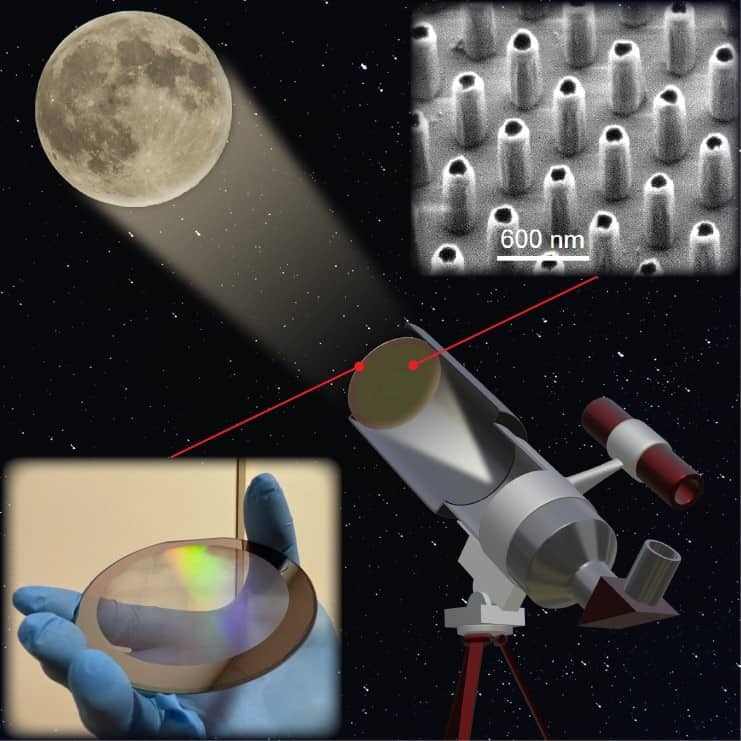
Future telescope: photomontage showing the metalens (bottom left) and part of its microscopic structure (upper right). Also shown is an image of the moon (not taken by the metalens) and an artistic impression showing how the metalens was used in a telescope. (Courtesy: Lidan Zhang et al/ACS Nano Letters)
An important step towards the practical use of optical metasurfaces has been taken by researchers in the US. The team used a common semiconductor manufacturing process to produce a large aperture, flat metalens. Its optical performance was demonstrated by using it as the objective lens in a simple telescope that was aimed at the Moon. The telescope achieved superior resolving power and produced clear images of the surface of the Moon.
Telescopes have been used to peer out into the universe for more than 400 years. In the early 1600s, Galileo Galilei used a telescope to observe the moons of Jupiter and last year the James Webb Space Telescope began taking spectacular images of the cosmos.
The telescopes used today by professional astronomers tend to be large and bulky, which often puts limits on how and where they can be used. The size of these instruments is a result of their large apertures and often-complicated multi-element optical systems that are necessary to eliminate aberrations and to provide the desired high performance.
Engineered nanostructures
Optical metasurfaces offer a potential way to make telescopes and other optical systems smaller and simpler. These are engineered nanostructures that can be thought of as a series of artificial optical antennas (see figure). These antennas can manipulate light, changing, for example, its amplitude, phase, and polarization.
These metasurfaces can be engineered to focus light, thereby creating metalenses that can offer significant advantages over conventional optics. For example, the flat surfaces of metalenses are free of spherical aberrations and metalenses are ultrathin and low in weight when compared to conventional optics.
However, the production of metalenses is still in its infancy. Current fabrication methods are based on scanning systems such as electron-beam (e-beam) lithography and focused ion beam (FIB) techniques. These are slow, expensive, and restrict the size of metalenses to just a few millimetres. This makes large-volume production almost impossible and means that metalenses are currently expensive and too small for the large-aperture applications such as telescopes.
A meta-telescope
Now, researchers at Pennsylvania State University and the NASA-Goddard Space Flight Center have come up with a much better way of making metalenses. Their process can be scaled up for large-scale production and can be used to create metalenses with large aperture sizes that are suitable for telescope applications.
The team used deep-ultraviolet (DUV) lithography, which is a technique commonly used in the semiconductor industry. Their process involved patterning the top of a four-inch silica wafer. Their 80-mm-diameter meta-lens was divided into 16 parts that were combined by exposing the same patterns on different quadrants of the wafer. Pattern stitching and wafer rotation eliminated the need for an expensive single large mask that exposes the entire surface.
Intensity profile
The performance of the metalens was characterized by measuring the intensity profile of focused laser beams over a broad wavelength range spanning 1200–1600 nm. The tests showed that the metalens can tightly focus light close to the diffraction limit over the entire range, despite being designed to operate at 1450 nm. However, diffractive dispersion did vary the focal length throughout the wavelength range – a detrimental effect called chromatic aberration.
The resolving power of the metalens was tested by using it as an objective lens inside a telescope. The team used the telescope to successfully image various features of the Moon’s surface with a minimum resolving feature size of approximately 80 km. This is the best reported resolving power for this type of metalens so far.
Next-generation systems
Lead researcher Xingjie Ni at Pennsylvania State University believes that metasurfaces can be a game changer in optics, because their unprecedented capability for light manipulation makes them powerful candidates for next-generation optical systems. This, he says, is why his team is dedicated to advancing the capabilities of scalable, fabrication-friendly metasurfaces.
“We plan to improve our design techniques to achieve fabrication-imperfection-tolerant nanostructures. This will allow us to use high-volume manufacturing technology such as photolithography to make large scale metalenses working in the visible range and incorporate more complex nanoantenna designs, for example, freeform shaped nanoantennas, to compensate for chromatic aberration,” he tells Physics World.
Din Ping Tsai at the City University of Hong Kong was not involved in the research and he thinks that this work expands the working scenarios of metalenses and will inspire research on metalenses with large apertures. He says that DUV lithography could be used to achieve the high throughput manufacturing of low cost metalenses with reasonable resolution. This would bring the components into commercialization and make them part of our daily life in the coming years.
Tsai believes that the chromatic aberration in the Penn State metalens limits its use to monochromatic applications. He also points out that the design of large-area broadband achromatic meta-lens is still a big challenge and is in strong demand. In addition, he believes that a large mask is the preferred way to make metalenses in order to avoid stitching errors and to simplify the fabrication process.
Quelle: Physics World
